Search for:
microLED GaN wafer
GaN microLED wafer (courtesy Creative Commons & Plessey Semiconductors)

MicroLED wafer inspection and defect review is crucial to the development and manufacturing scale-up of display devices for consumer AR devices and commercial head-up displays.

InZiv

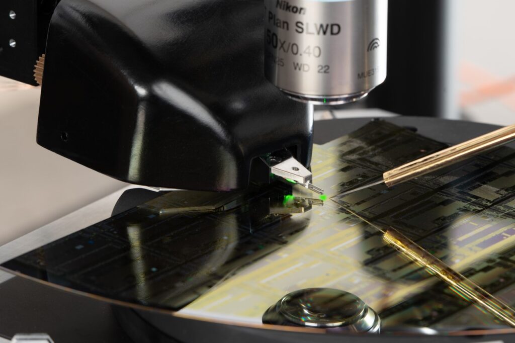
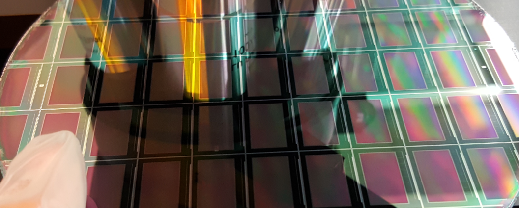
Corbeau Innovation’s partner InZiv has developed a state-of-the-art microLED wafer inspection system. The OmniPix 2.0 combines automated optical inspection, PL and EL over whole wafers up to 12″ and 100 nm resolution defect inspection in the same instrument.

spatial resolution 100 nm

OmniPix-ML1000 nano PL & EL
Microelectronics

Measure

  • Whole wafer AOI PL and EL

  • Individual pixel PL and EL resolution

  • Individual pixel External Quantum Efficiency
  • Individual pixel angular emission function
  • Individual pixel spectral and lifetime emission
  • Individual pixel sidewall measurement

Corbeau Innovation Ltd is the authorised representative of InZiv in the United Kingdom and Nordic regions